
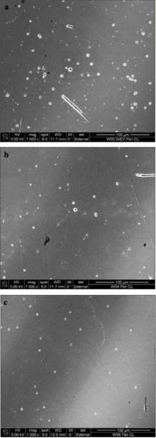
The approach used to meet the project objectives was to start with low-dislocation-density aluminum nitride (AlN) single-crystal substrates and grow graded AlxGa1-xN layers on top.
Pseudomorphic AlxGa1-xN epitaxial layers grown on bulk AlN substrates were used to fabricate LEDs and demonstrate better device performance as a result of the low defect density in these layers when bench-marked against state-of-the-art LEDs fabricated on sapphire substrates. The pseudomorphic LEDs showed excellent output powers compared to similar wavelength devices grown on sapphire substrates, with lifetimes exceeding 10,000 hours (which was the longest time that could reliably be estimated). In addition, high internal quantum efficiencies were demonstrated at high driving current densities even though the external quantum efficiencies were low due to poor photon extraction. Unfortunately, these pseudomorphic LEDs require high aluminum content so they emit in the ultraviolet (UV). Sapphire-based LEDs typically have threading dislocation densities (TDD) > 108 cm-2 while the pseudomorphic LEDs have TDD ≤ 105 cm-2. The resulting TDD, when grading the AlxGa1-xN layer all the way to pure GaN to produce a GaN-ready substrate, has varied between the mid 108 down to the 106 cm-2. An approach to improve the LED structures on AlN substrates for light extraction efficiency was developed by thinning and roughening the substrate.
Overall, the use of pseudomorphic epitaxial growth for the fabrication of LEDs allowed for improved performance of the device. This improvement is due to the considerably lower defect density determined on pseudomorphic layers as opposed to defect density measured on relaxed layers. This attribution is confirmed by comparing the performance of similar emission wavelength devices grown on AlN and sapphire at different drive current density, reaching up to 400 A/cm2. The external quantum efficiency for pseudomorphic LEDs is higher and flatter than that determined for sapphire-based devices with similar composition, and shows a very similar trend to that of commercial InGaN-based light-emitting diodes.
The goal of developing a cost-effective approach to generate low-dislocation density GaN substrates based on AlN was hindered by two drawbacks: Crystal IS has demonstrated high-quality, crack-free, 2-inch AlN substrates, but has not developed a consistent, high-yield product. The second critical barrier is the question of how high the gallium concentration in the AlxGa1-xN buffer layer can be pushed while maintain- ing a low TDD. Higher Ga concentrations will be needed for near-UV or visible blue LEDs. While this work suggests that low TDD are possible in epitaxial layers grown on AlN substrates even with pure GaN, these results have been difficult to reproduce across the large areas needed for cost-effective LED manufacture.
Once these hurdles are surmounted, the use of a platform conducive to lower defect density in the epitaxial layers will be reflected in the performance of LEDs with emission wavelength in the visible, as well as they are already reflected in the performance of UV LEDs.
This work was done by Sandra B. Schujman and Leo J. Schowalter of Crystal IS, Inc.
This Brief includes a Technical Support Package (TSP).
GaN-Ready Aluminum
(reference GDM0016) is currently available for download from the TSP library.
Don't have an account?
Overview
The document presents a comprehensive report on a project focused on the development of low defect density substrates for III-nitride light-emitting diodes (LEDs), specifically targeting the growth of AlInGaN-based devices. The primary objectives were to investigate the relationship between threading dislocation density and device performance, and to create a cost-effective method for generating low-defect substrates suitable for visible light-emitting diodes.
The project revealed that while the connection between low defect density and device performance was not initially clear for nitride-based LEDs, it was established that the lifetime of nitride laser diodes improved with decreasing defect density. A significant breakthrough was achieved by Crystal IS, which demonstrated the possibility of growing pseudomorphic epitaxial layers of AlxGa1-xN on AlN substrates with thicknesses far exceeding those predicted by equilibrium theories. Specifically, layers of Al0.7Ga0.3N and Al0.6Ga0.4N were successfully grown without relaxation, providing a promising platform for testing the performance of LEDs.
The report details experimental methods and results, highlighting the performance of devices under different conditions. For instance, it was noted that under pulsed conditions, devices could achieve output powers exceeding 15 mW at injection current densities of 400 A/cm², with minimal degradation in external quantum efficiency (EQE). In contrast, devices operated in continuous mode exhibited a significant decrease in EQE at lower current densities.
Despite the successes in understanding device performance, the project faced challenges in consistently obtaining substrates with diameters compatible with industry fabrication tools for InGaN-based LEDs. The report emphasizes the importance of reducing substrate thickness to minimize optical losses, with reductions down to 20 µm or 10 µm potentially decreasing losses to less than 5%.
Overall, the findings contribute valuable insights into the optimization of nitride-based LEDs, particularly in terms of substrate quality and its impact on device performance. The research underscores the potential for improved efficiency and longevity in LED technology, paving the way for advancements in solid-state lighting applications. The document concludes with a roadmap for future developments in aluminum nitride substrates and their role in enhancing solid-state lighting technologies.