
An improved method of fabrication of cathodes of microbatteries is based on electrophoretic deposition. Heretofore, sputtering (for deposition) and the use of photoresist and liftoff (for patterning) have been the primary methods of fabricating components of microbatteries. The volume of active electrode material that can be deposited by sputtering is limited, and the discharge capacities of prior microbatteries have been limited accordingly. In addition, sputter deposition is slow. In contrast, electrophoretic deposition is much faster and has shown promise for increasing discharge capacities by a factor of 10, relative to those of microbatteries fabricated by prior methods.
Microbatteries of the type to which the improved method applies are fabricated on silicon wafers, with cell footprints of the order of (50 to 100 μm)2. In the improved method, cathodes are formed directly on cathode current-collector pads; there is no need for additional lithography or etching to define the cathodes. In order to make it possible for cathode material to be deposited onto current-collector pads, it is necessary to ensure that the pads are electrically connected to ground during the electrophoretic deposition process. This can be done in any of several different ways. For example, current collectors can be deposited by sputtering and patterned such that a metal line connects all current collectors. After electrophoretic deposition of cathode material, the connecting lines can be removed by simple patterning and etching to yield unconnected microbattery cells.
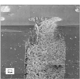
A suspension of powdered cathode material (e.g., LiCoO2), acetone, iodine, and an electrically conductive additive is prepared. The iodine serves to facilitate the formation of positively charged complexes of the particles to be deposited so that they can be moved through the applied electric field during deposition. The conductive additive could be, for example, tin powder or carbon black.
The substrate is positioned about 1 cm from a counter electrode. The substrate/counter-electrode assembly is immersed in the suspension, and then a potential of about 70 V is applied between the substrate and the counter electrode (the counter electrode being positive with respect to the substrate) for a time of about 90 seconds. The particles of cathode material, being positively charged, are transported through the suspension to the silicon substrate, where they become deposited only on electrically conductive surfaces. The substrates are then coated with a solid-electrolyte film and patterned with anode current collectors by use of previously published techniques.
This work was done by William West, Jay Whitacre, and Ratnakumar Bugga of Caltech for NASA's Jet Propulsion Laboratory. For further information, access the Technical Support Package (TSP) free on-line at www.nasatech.com/tsp under the Manufacturing category.
n accordance with Public Law 96-517, the contractor has elected to retain title to this invention. Inquiries concerning rights for its commercial use should be addressed to
Intellectual Assets Office
JPL
Mail Stop 202-233
4800 Oak Grove Drive
Pasadena, CA 91109
(818) 354-2240
E-mail:
Refer to NPO-30394, volume and number of this NASA Tech Briefs issue, and the page number.
This Brief includes a Technical Support Package (TSP).
Electrophoretic Deposition for Fabricating Microbatteries
(reference NPO-30394) is currently available for download from the TSP library.
Don't have an account?
Overview
The document discusses a novel method for fabricating microbatteries, specifically designed for applications in micro/nanospacecraft, utilizing electrophoretic deposition (EPD). This technique addresses the limitations of traditional microbattery fabrication methods, which often struggle with low capacity due to the restricted amount of active material that can be deposited in a small area.
Microbatteries are fabricated on silicon wafers with cell footprints ranging from 50 to 100 μm². The new method allows for the direct formation of cathodes on current-collector pads, eliminating the need for additional lithography or etching processes. This is achieved by ensuring that the current-collector pads are electrically connected to ground during the EPD process. The document outlines two approaches for achieving this: one involves sputtering current collectors and patterning them, while the simpler method uses an electrically conductive silicon substrate coated with an insulating layer, which is then patterned to create vias for the cathode current collectors.
The capacity of these microbatteries is primarily limited by the thickness and area of the cathode film. Current techniques restrict cathode film thickness to about 0.25 to 0.5 μm, which can lead to challenges such as heating and hardening of photoresist during sputtering, making liftoff difficult. The new EPD method allows for the rapid deposition of thicker cathode materials, such as LiCoO₂ or V₂O₅, which can significantly enhance battery performance.
The document emphasizes the potential of this new fabrication process to produce microbatteries with approximately ten times higher capacity and a flatter discharge voltage profile compared to existing methods. This advancement is particularly relevant for the miniaturization of spacecraft components, where integrated power sources can reduce mass and improve efficiency in wiring and packaging.
Overall, the document highlights the innovative approach to microbattery fabrication that could enable a wider range of applications in commercial, aerospace, and military fields, facilitating distributed sensing and exploration missions. The work was conducted under the auspices of NASA and the Jet Propulsion Laboratory, showcasing the potential for significant advancements in energy storage technology.