
The figure depicts two digital waveforms and a block diagram of a digital phase meter for measuring the difference between their phases. This digital phase meter is being developed for incorporation into a laser heterodyne interferometer in a metrological apparatus, but could also be adapted to other uses. Relative to prior phase meters of similar capability, including digital ones, this digital phase meter is smaller, less complex, and less expensive. The phase meter has been constructed and tested in the form of a field-programmable gate array (FPGA) of fewer than 104 gates.
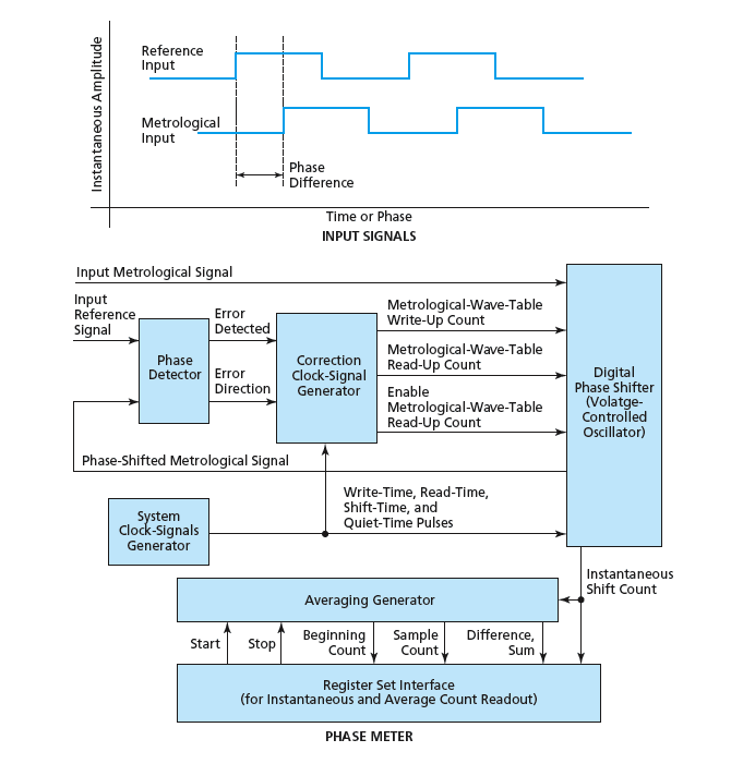
The three main components at the heart of the phase meter are a phase detector, a correction clock-signal generator, and a digital phase shifter. These components are connected to form a phase-locked loop (PLL) that is a slightly modified version of a conventional PLL. The modification consists mainly in feeding the metrological input signal, instead of the reference input signal, to one of the input terminals of the phase shifter. That is to say, whereas the phase of the reference signal gets shifted in a conventional PLL, the phase of the metrological signal is the one that gets shifted in this PLL.
The reference signal is fed to one of the two inputs of a phase detector, while the phase-shifted metrological signal is fed to the other input of the phase detector, which measures the difference between the phases of its inputs and puts out a correction command (basically, a pair of error feedback signals) in an effort to drive the difference toward zero. The correction command is fed to the correction clock-signal generator, the outputs of which are fed as inputs to the digital phase shifter. The overall action of the loop is to shift the phase of the metrological signal until it becomes phase-aligned with the reference signal. When this alignment is achieved, the phase detector stops sending correction commands to the phase shifter.
One of the outputs of the phase detector is a number proportional to the instantaneous phase shift imposed on the metrological signal. This number is fed to an averaging generator and a register set interface for display of instantaneous and time-averaged phase readings, which can include readings from which initial values have been subtracted so as to indicate the change in phase shift from the initial to the current or final state of a metrological process.
This work was done by Frank Loya of Caltech for NASA's Jet Propulsion Laboratory.
NPO-40318
This Brief includes a Technical Support Package (TSP).
Digital Phase Meter for a Laser Heterodyne Interferometer
(reference NPO-40318) is currently available for download from the TSP library.
Don't have an account?
Overview
The document is a Technical Support Package from NASA's Jet Propulsion Laboratory (JPL) detailing the development of a Digital Phase Meter for a Laser Heterodyne Interferometer, identified as NPO-40318. This technology is part of NASA's Commercial Technology Program, aimed at disseminating aerospace-related advancements with broader technological, scientific, or commercial applications.
The Digital Phase Meter is designed to enhance the precision of measurements in laser interferometry, a technique widely used in various scientific fields, including astrophysics and metrology. The document outlines the technical specifications and operational principles of the device, emphasizing its ability to achieve high phase resolution, approaching 10^-6 fringe cycle counts.
Key components of the system include an Altera Acex model EP1K30TC144-3 FPGA, which serves as the core processing unit. The design incorporates a Heterodyne Interferometer Simulator that allows for adjustable phase offsets of up to 180 degrees at 100 kHz. The initial prototype utilized a commercial 50 MHz CMOS clock IC, with plans to upgrade to a precision clock source for improved accuracy.
The document also describes the architecture of the Digital Phase Shifter, which is a critical component of the system. This module must maintain a live digital representation of the incoming metrology signal, provide outputs without phase errors, and accurately count phase-shifting events. The phase shifter employs dual-port bit memory to store incoming signals, with a limited capacity of 2048 or 4096 bits, necessitating careful management of wave storage to avoid rollover errors.
Additionally, the phase detector and correction signal generator are discussed, highlighting their roles in synchronizing the system and filtering noise. The design aims to minimize technical issues encountered in earlier prototypes, ensuring a purely digital operation in future iterations.
Overall, the document serves as a comprehensive overview of the Digital Phase Meter's design, functionality, and potential applications, showcasing JPL's commitment to advancing metrology technologies. For further inquiries or collaboration opportunities, the document provides contact information for the Innovative Technology Assets Management office at JPL.