
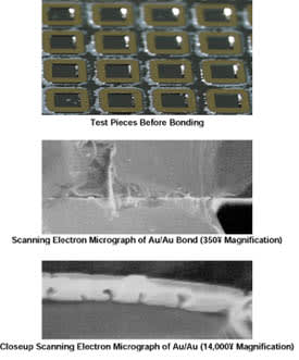
Microwave heating is the basis of a simple technique for quickly and gently bonding two metallized dielectric or semiconductor wafers to each other. The technique can be used, for example, to bond a flat, gold-coated silicon wafer to another gold-coated silicon wafer that is flat except for a cavity, in order to hermetically seal the cavity (see figure). The technique has the potential to become a standard one for bonding in the fabrication of microelectromechanical systems (MEMS).
The predecessor of this technique is thermocompression bonding, in which two substrates to be bonded are clamped together with considerable pressure and the entire resulting assembly is heated to melt eutectic metal alloy coats on the faying substrate surfaces. (Even though elemental metals could be more desirable under some circumstances, eutectics are used because they have lower melting temperatures.) The bonding process can take as long as 24 hours. The heat and pressure can degrade the product; the degradation can include deleterious effects of clamping stresses, diffusion of the metal into the substrate material, and diffusion of substrate material into the metal bond.
In the present technique, bonding could be effected in a few seconds, with minimal or no clamping, and without heating the entire assembly. Two pieces to be bonded are simply placed (e.g., one atop the other), in a microwave cavity. The position and orientation of the pieces in the microwave cavity is chosen to optimize coupling of the metal in the bond with the electromagnetic mode that is to be excited in the microwave cavity. The microwave cavity is evacuated to prevent the formation of a plasma. A pulse of microwave power (typically a few hundred watts for a few seconds) is applied.
Because the substrates are nearly transparent to microwaves in the presence of metal layers, heating by the microwave field is concentrated in the metal layers in the bond region. More precisely, by virtue of the electromagnetic skin effect, most of the deposition of electromagnetic energy occurs within a skin depth ≈1 µm at microwave frequencies) at the surface of the metal. Thus, heating is concentrated exactly where it is needed — at the interface between the two metal layers that one seeks to melt together. By the time the pulse is turned off, the metal layers have been melted together, yet the substrates remain cool. Of course, heat is conducted from the interface to adjacent depths, but the resulting heating of the substrate is transient and minimal — not enough to cause appreciable diffusion of metal or substrate material.
The figure depicts some aspects of silicon workpieces that were fabricated and tested to demonstrate the present technique. Each piece started as 5-mm square silicon wafer. A strip 2 mm wide around the edge of one face of each piece was coated with Cr to a thickness of 150 Å, then Au to a thickness of 1,200 Å. The gold coat was to serve later as the bonding metal. Each piece was etched to form 3-by-3-mm, 100-µm-deep recess in the middle of one face; the recess was to become half of a hermetically sealed cavity. Then pairs of these pieces were bonded to form the hermetically sealed cavities. In a test of their hermeticity, the bonded pairs were found to leak at low rates comparable to the background level of a leak-measuring mass spectrometer.
This work was done by Nasser Budraa, Martin Barmatz, John Mai, Tom Pike, and Henry Jackson of Caltech for NASA's Jet Propulsion Laboratory. For further information, access the Technical Support Package (TSP) free on-line at www.nasatech.com/tsp under the Manufacturing & Prototyping category.
This invention is owned by NASA, and a patent application has been filed. Inquiries concerning nonexclusive or exclusive license for its commercial development should be addressed to
the Patent Counsel
NASA Resident Office–JPL; 818-354-4770.
Refer to NPO-20608.
This Brief includes a Technical Support Package (TSP).
Hermetic Water Bonding by Use of Microwave Heating
(reference NPO-20608) is currently available for download from the TSP library.
Don't have an account?
Overview
The document presents a novel microwave bonding technology developed by researchers at the Jet Propulsion Laboratory (JPL), California Institute of Technology, aimed at enhancing the fabrication of Micro Electro-Mechanical Systems (MEMS). This innovative method utilizes microwave radiation to bond gold on silicon substrates (Au/Si) efficiently, addressing challenges associated with traditional bonding techniques.
The key advantage of this microwave bonding process is its ability to selectively heat materials, concentrating energy in the metallic portions of the substrates while minimizing the heating of the silicon. This selective heating occurs within a skin depth of approximately 1 micrometer, allowing for rapid bonding without the application of mechanical pressure, which reduces the risk of inducing mechanical stresses in the materials. As a result, the bonded substrates form hermetically sealed micron-sized cavities, crucial for the functionality and reliability of MEMS devices.
Preliminary tests, including helium fine leak tests, indicate that the bonded samples exhibit low leak rates, suggesting that the cavities can maintain their integrity for extended periods—estimated at around 1.2 years before returning to standard atmospheric pressure. This is particularly significant for applications where maintaining a vacuum or controlled environment is essential.
The document highlights the limitations of existing bonding methods, such as anodic bonding, thermocompression, and polymer adhesives, which often involve longer processing times and potential degradation of materials. In contrast, the microwave bonding technique can achieve successful bonds in a matter of seconds, significantly improving the efficiency of MEMS fabrication.
Furthermore, the technology is positioned as a potential standard process in the MEMS industry, leveraging the existing infrastructure of the silicon industry to facilitate widespread adoption. The authors emphasize the importance of this advancement in the context of the anticipated technological revolution in MEMS, which are expected to find applications across various scientific and commercial fields.
In summary, this document outlines a groundbreaking approach to wafer bonding that promises to enhance the quality, speed, and reliability of MEMS fabrication, thereby contributing to the future of microtechnology and its applications.