Stories
34,35
0
270
30
Application Briefs: Photonics/Optics
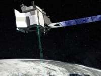
New satellites equipped with Corning’s advanced hyperspectral-imaging technology can detect pipeline leaks and other environmental issues, providing precise monitoring and exploration capabilities for businesses and governments.
Application Briefs: Photonics/Optics
Optical parametric oscillator (OPO) lasers have long been utilized in sophisticated test and measurement applications such as mass spectrometry, photoacoustic imaging, and spectroscopy.
Articles: Photonics/Optics
The blue laser has become the ideal light source for high-reflective metal processing, offering substantial advantages in various industrial applications such as cutting and welding.
Articles: Materials
Any plan for the long-term exploration or habitation of the Moon and Mars will almost certainly entail the use of multiple habitats, vehicles and remotely located equipment, all of which will require power sources.

Blog: Manufacturing & Prototyping
Choosing a present for an engineer is almost as daunting as performing the tasks of an engineer. With that in mind, we here at Tech Briefs aim to make your life easier with regards to the former.

Blog: Photonics/Optics
A new laser-based technique could speed up the discovery of promising metamaterials for real-world applications.
Special Reports: Imaging

ADAS/Connected Car - December 2023
In this compendium of popular articles from the editors of Automotive Engineering and ADAS & Autonomous Vehicle Engineering magazines, see how advances in simulation, testing, lidar/sensors, displays, and...Briefs: Test & Measurement
Processes and structures within the body that are normally hidden from the eye can be made visible through medical imaging. Scientists use imaging to investigate...
Briefs: Imaging
Researcher are finding ways to estimate a target location when light gets deflected by a disordered structure.
Briefs: Imaging
Imagine being able to snap a picture of extremely fast events on the order of a picosecond.

Briefs: Materials
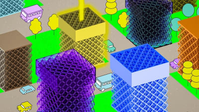
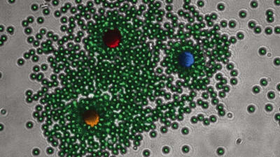
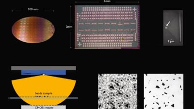
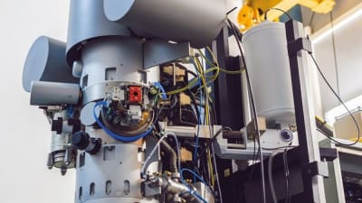
To further shrink electronic devices and to lower energy consumption, the semiconductor industry is interested in using 2D materials but manufacturers need a quick and accurate method for detecting defects in these materials to determine if the material is suitable for device manufacture.
Briefs: Photonics/Optics
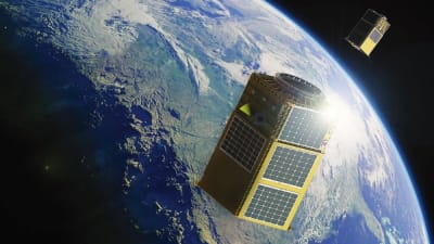
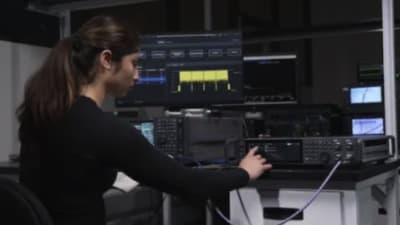
Making Satellite, Ground Communication More Effective
Rensselaer Polytechnic Institute’s Moussa N’Gom has devised a method to make communications between satellites and the ground more effective — regardless of the weather.
Products: Software
See the new products, including new Vision hardware from Beckhoff; Renishaw’s new Central manufacturing connectivity and data platform; Weidmuller USA's new open operating system, u-OS; a Digital Valve Controller featuring the Device™ technology; and more.

Briefs: Photonics/Optics
MIT researchers have developed a camera-based touch sensor that is long, curved, and shaped like a human finger. Their device provides high-resolution tactile sensing over a large area. The sensor, called the GelSight Svelte, uses two mirrors to reflect and refract light.
Special Reports: Aerospace

Space Technology - November 2023
Read about NASA's plans for future Mars exploration, ultrafast laser-based space communications, new strategies for cleaning up orbital debris, and much more in this compendium of recent articles from the...Products: Design
These 12 products are the nominees for the 2020 Tech Briefs Readers’ Choice Product of the Year.
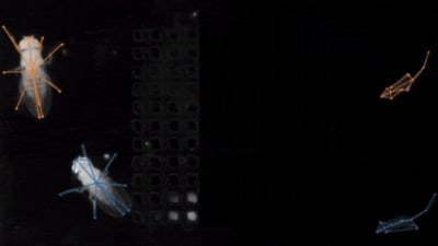
Blog: Imaging
The desire to understand how the brain generates and patterns behavior has driven rapid methodological innovation in tools to quantify natural animal behavior.
Special Reports: Power

EV Battery Innovation - November 2023
Read about the latest advances in EV battery testing, fast-charging, materials technology, and much more in this new report brought to you by Battery & Electrification Technology and Automotive...Briefs: Materials
Researchers have developed a viable dust, water, and ice mitigation optical coating for space flight, aeronautical, and ground applications. The innovation of the LOTUS coating prevents contamination on sensitive surfaces.
Briefs: Materials
Researchers from Imperial College London and University College London have demonstrated the first spontaneously self-organizing laser device, which can reconfigure when conditions change.
Briefs: Photonics/Optics
Researchers at the University of California San Diego have developed soft devices containing algae that glow in the dark when experiencing mechanical stress, such as being squished, stretched, twisted, or bent.

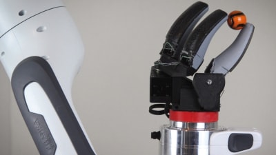
Briefs: Robotics, Automation & Control
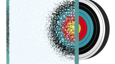
Research reveals that expertly timed lasers shined at an approaching LIDAR system can create a blind spot in front of the vehicle.

Application Briefs: Photonics/Optics
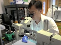
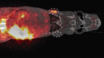
Researchers from MIT Lincoln Laboratory and their collaborators at the Massachusetts General Hospital Center for Ultrasound Research and Translation have developed a new medical imaging device: the Noncontact Laser Ultrasound (NCLUS).

Articles: Imaging
Engineers developing products or systems incorporating thermal cameras need to clearly understand the critical design specifications, including scene dynamic range, field of view, resolution, sensitivity, and spectral range, to name a few.

Articles: Materials
Chalcogenide materials have emerged as a disruptive force in the optics industry, significantly enhancing optical performance in response to germanium export constraints. Their exceptional optical properties, adaptability, and precision engineering capabilities position them as invaluable assets for top optical performance.

Products: Photonics/Optics
See the new products, including CamTest TempControl from TRIOPTICS,
Semtech Corporation's Transimpedance Amplifiers, Kaman Precision Products' ThreadChecker, Keysight Technologies' oscilloscopes, and more.
Briefs: Communications
Researchers have outlined a new optical communication protocol that exploits spatial patterns of light for multi-dimensional encoding in a manner that does not require the patterns to be recognized, thus overcoming the prior limitation of modal distortion in noisy channels.
Briefs: Imaging
Researchers have developed the world’s smallest LED. It enables the conversion of existing mobile phone cameras into high-resolution microscopes. Smaller than the wavelength of light, the new LED was used to build the world’s smallest holographic microscope.
Briefs: Lighting
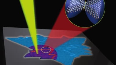
With a new microscopy technique that uses blue light to measure electrons in semiconductors and other nanoscale materials, a team of researchers is opening a new realm of possibilities in the study of these critical components, which can help power devices like mobile phones and laptops.
Top Stories
 Blog: Design
A Stretchable OLED that Can Maintain Most of Its Luminescence
 INSIDER: Design
Advancing All-Solid-State Batteries
 Blog: Power
My Opinion: We Need More Power Soon — Is Nuclear the Answer?
 Blog: Energy
Batteries that Can Withstand the Cold
 Quiz: Power
 Blog: Robotics, Automation & Control
Microscopic Swimming Machines that Can Sense, Respond to Surroundings
Webcasts
 On-Demand Webinars: Transportation
Advantages of Smart Power Distribution Unit Design for Automotive &...
 Upcoming Webinars: Unmanned Systems
Quiet, Please: NVH Improvement Opportunities in the Early Design...
 Upcoming Webinars: AR/AI
From Spreadsheets to Insights: Fast Data Analysis Without Complex...
 Upcoming Webinars: Electronics & Computers
Cooling a New Generation of Aerospace and Defense Embedded...
 Upcoming Webinars: AR/AI
Beyond AI-Copy-Paste Engineering: Advanced AI-Integration Success...