
-1
180
30
Articles: Medical
See the products of tomorrow, including a new type of 3D-printed titanium that’s about a third cheaper than commonly used titanium alloys; specially designed metasurfaces — flat devices etched with nanoscale light-manipulating patterns — to act as ultra-thin upgrades for quantum-optical chips and setups; and a handheld slide staining system designed to support medical, research, or environmental monitoring.
Products: Information Technology
See the product of the month: Phoenix Contact's NearFi, a contactless real-time transmission technology.

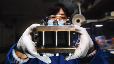
Q&A: Green Design & Manufacturing
Shu Yang and her materials research team at the University of Pennsylvania, along with the architect Masoud Akbarzadeh, Director of the Polyhedral Structures Laboratory, have developed a 3D-printed concrete based on diatomaceous earth that has enhanced carbon capture, is strong, and uses less CO2-producing cement.

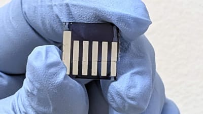
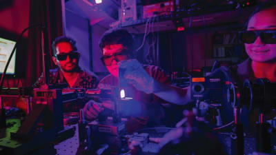
5 Ws: Photonics/Optics
North Carolina State University engineers have built a tiny spectrometer that is orders of magnitude smaller than current technologies and can accurately measure wavelengths of light from ultraviolet to the near infrared.
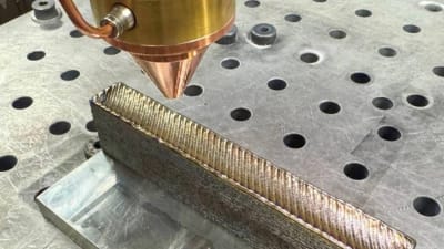
NASA Spinoff: Materials
AI SpaceFactory sells 3D printers informed by its work on Marshall Space Flight Center’s Centennial Challenge, which the company won with print material containing crushed basalt similar to ground cover on Mars.

Application Briefs: Software
Why should you know the right trigger strategy? Read on to find out.

Briefs: Imaging
Metabolic imaging is a noninvasive method that enables clinicians and scientists to study living cells using laser light, which can help them assess disease progression and treatment responses. But light scatters when it shines into biological tissue, limiting how deeply it can penetrate and hampering the resolution of captured images. Now, MIT researchers have developed a new technique that more than doubles the usual depth limit of metabolic imaging. Read on to learn more.

Briefs: Green Design & Manufacturing
AI systems like ChatGPT are notorious for being power-hungry. To tackle this challenge, a team from the Centre for Optics, Photonics and Lasers has come up with an optical chip that can transfer massive amounts of data at ultra-high speed. As thin as a strand of hair, this technology offers unrivaled energy efficiency. Read on to learn more.
Briefs: Photonics/Optics
As fast as modern electronics have become, they could be much faster if their operations were based on light, rather than electricity. Fiber optic cables already transport information at the speed of light, but to do computations on that information without translating it back to electric signals will require a host of new optical components. Researchers have now developed such a device. Read on to learn more.
Briefs: Photonics/Optics
Engineers at the University of California San Diego have achieved a long-sought milestone in photonics: creating tiny optical devices that are both highly sensitive and durable — two qualities that have long been considered fundamentally incompatible. Read on to learn more.
Briefs: Photonics/Optics
Researchers have invented a new type of tunable semiconductor laser that combines the best attributes of today’s most advanced laser products, demonstrating smooth, reliable, wide-range wavelength tuning in a simple, chip-sized design. Read on to learn more about it.

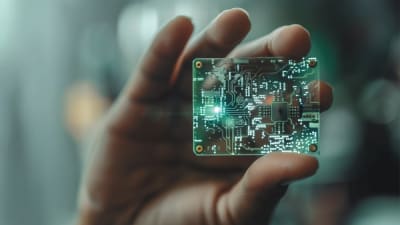
Products: Electronics & Computers
See the new products, including Corning Incorporated's Corning® Gorilla® Glass Ceramic; Epoxy Technology's EPO-TEK®353NDP, a high-performance, humidity-resistant epoxy; Edmund Optics' off-the-shelf HOLO/OR Diffractive Diffusers and Beamsplitters; Teledyne Technologies subsidiary FLIR's advanced multispectral imaging solution; and much more.
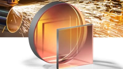
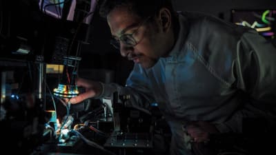
Articles: Photonics/Optics
DPSS lasers are a critical enabling technology for meeting the precision materials processing demands of advanced packaging. Both nanosecond and USP lasers can achieve excellent results, but the right choice depends on specific requirements. Read on to learn more.

Articles: Imaging
Patent-pending imaging technologies created in Purdue University’s College of Engineering could be developed and commercialized for applications as diverse as medical imaging, autonomous navigation, surveillance, microscopy, and advanced manufacturing. Read on to learn more about it.

Application Briefs: Electronics & Computers
For loading and unloading workpiece carriers containing wafers of different sizes in an automated process prior to PECVD coating, acp systems has developed a robotic solution aided by image processing for a leading manufacturer of space solar technology. Read on to learn more.

Articles: Software
This article briefly examines why isolation is required, emphasizing the need in sensor-based circuits. It then looks at various aspects of isolation using state-of-the-art digital isolators from Analog Devices and shows how they can be applied.
Articles: Energy
In-space manufacturing is expected to become a core part of future space economy by using assets in orbits or beyond Earth orbit for use in space. Tech Briefs interviewed space-focused solar energy startup Solestial’s CTO Stanislau Herasimenka about the key technology developments leading to this increased momentum for space-based manufacturing and the role solar power will play in it. Read on for the full interview with Herasimenka, edited for length and clarity.

Briefs: Power
NASA researchers are eliminating complex joints by manufacturing a 1-piece TCA utilizing 3D printing and large-scale additive manufacturing technologies to directly deposit the nozzle onto the combustion chamber. And, by replacing a traditional solid metal jacket with a composite overwrap for support, the overall weight is reduced by over 40 percent. Read on to learn more.

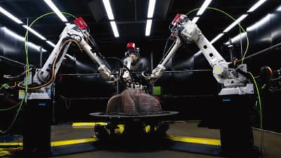
Briefs: Manufacturing & Prototyping
Researchers at the Department of Energy’s Oak Ridge National Laboratory are using advanced manufacturing techniques to revitalize the domestic production of very large metal parts that weigh at least 10,000 pounds each and are necessary for a variety of industries, including clean energy. Read on to learn more.
Briefs: Materials
MIT researchers have used 3D printing to produce self-heating microfluidic devices, demonstrating a technique which could someday be used to rapidly create cheap, yet accurate, tools to detect a host of diseases. Read on to learn more.

Briefs: Photonics/Optics
Researchers have developed an on-chip twisted moiré photonic crystal sensor that uses MEMS technology to control the gap and angle between the crystal layers in real time. The sensor can detect and collect detailed polarization and wavelength information simultaneously. Read on to learn more.

Briefs: Imaging
Engineers at NASA Langley Research Center have developed a cutting-edge thermal inspection technology that enhances defect detection on low-emissivity surfaces by eliminating false readings caused by infrared reflections. Read on to learn more.

Briefs: Wearables
Virtual reality video games that combine screen time with exercise are a great way to get fit, but game designers face a major challenge — adherence to ‘exergames’ is low, with most users dropping out once they start to feel uncomfortable or bored. Read on to learn what a team did to thwart this.

Briefs: Manned Systems
Innovators at NASA Johnson Space Center have developed a thin film sensor that measures temperatures up to 1200 °F, and whose prototype successor may achieve measurements up to ~3000 °F — which was the surface temperature of the Space Shuttle during its atmospheric reentry. Read on to learn more.

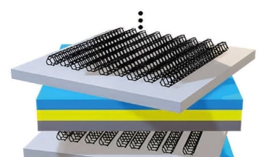
Briefs: Physical Sciences
A research team led by scientists at Lawrence Berkeley National Laboratory (Berkeley Lab) has developed a new fabrication technique that could improve noise robustness in superconducting qubits, a key technology for enabling large-scale quantum computers. Read on to learn more.

Briefs: Imaging
A new computer vision technique developed by MIT engineers significantly speeds up the characterization of newly synthesized electronic materials. The technique automatically analyzes images of printed semiconducting samples and quickly estimates two key electronic properties for each sample. Read on to learn more.

Briefs: Energy
Solar cells account for approximately six percent of the electricity used on Earth; however, in space, they play a significantly larger role, with nearly all satellites relying on advanced solar cells for their power. That’s why Georgia Tech researchers will soon be sending 18 photovoltaic cells to the International Space Station (ISS) for a study of how space conditions affect the devices’ operation over time. Read on to learn more.

Briefs: Power
For years, researchers have been developing tools to accelerate the materials discovery and development of new energy storage technologies, including those that can predict the performance of the batteries systems for long-term grid services. With a new physics-based simulation tool, EZBattery Model, it now takes less than a second to predict the performance of redox flow batteries and its variants. Read on to learn more.
Briefs: Power
Idle Trucks to Power the Grid with Clean Energy
University of Waterloo researchers are tapping into idled electric vehicles to act as mobile generators and help power overworked and aging electricity grids. Read on to learn more about it.
Top Stories
 Blog: Lighting
A Stretchable OLED that Can Maintain Most of Its Luminescence
 Blog: Energy
Batteries that Can Withstand the Cold
 INSIDER: Energy
Advancing All-Solid-State Batteries
 Quiz: Energy
 Blog: Physical Sciences
 Blog: Materials
Webcasts
 Upcoming Webinars: Sensors/Data Acquisition
From Spreadsheets to Insights: Fast Data Analysis Without Complex...
 Upcoming Webinars: Electronics & Computers
Cooling a New Generation of Aerospace and Defense Embedded...
 Upcoming Webinars: Sensors/Data Acquisition
Beyond AI-Copy-Paste Engineering: Advanced AI-Integration Success...
 Upcoming Webinars: Power
Battery Abuse Testing: Pushing to Failure
 Upcoming Webinars: Connectivity
A FREE Two-Day Event Dedicated to Connected Mobility
 Upcoming Webinars: Test & Measurement
Choosing the Right N-Port Strategy: Multiport VNAs vs. Switch...