Stories
54
0
120
30
Articles: Manufacturing & Prototyping
Future electric vehicles will be more efficient, more powerful, and will be able to hold more energy in their batteries than today’s EVs. Those big “mores” require countless small improvements beyond the headline component — batteries. Read on to learn more.
Articles: Electronics & Computers
Most PCB manufacturers use automatic optical inspection (AOI) to monitor defects in their printed circuit boards. This delivers strong results when there are defects in the soldering, connections, pads, and traces on printed boards.

Products: Software
See the product of the month: The new multi-purpose ICAM-B charge amplifier from Kistler, which is ideal for use with piezoelectric sensors.

Briefs: Materials
A research team from Kyushu University, in collaboration with Japanese company Nitto Denko, has developed a tape that can be used to stick 2D materials to many different surfaces, in an easy and user-friendly way.

Briefs: Energy
Microelectronics face a key challenge because of their small size. To avoid overheating, microelectronics need to consume only a fraction of the electricity of conventional electronics while still operating at peak performance. Researchers have achieved a breakthrough that could allow for a new kind of microelectronic material to do just that.
Articles: Robotics, Automation & Control
See the products of tomorrow, including a new DC-DC power converter developed by engineers at the Kobe University, a haptic device capable of reproducing the softness of various materials developed by EPFL researchers, and three-dimensional embroidery techniques from engineers from NC State University.

Special Reports: Materials
Advanced Materials & Coatings - May 2024
In this compendium of articles from the editors of Tech Briefs and Aerospace & Defense Technology, learn how breakthroughs in materials science are enabling exciting new applications in quantum...INSIDER: Photonics/Optics
Engineers at MIT, Nanyang Technological University, and several companies have developed a compact and inexpensive technology for detecting and measuring lead concentrations in water,...
INSIDER: Electronics & Computers
Researchers at the École Polytechnique Fédérale de Lausanne (EPFL) — or Swiss Federal Institute of Technology in Lausanne — have leveraged the use of...
Application Briefs: Photonics/Optics
Understanding how to effectively tolerance aspheres is an incredibly useful communication tool to get the most out of your lens. In this article, we will provide some context behind asphere tolerances, exploring the factors that influence cost and performance.

Briefs: Sensors/Data Acquisition
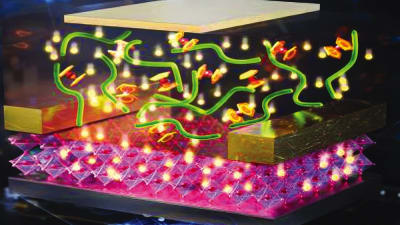
Researchers from Tokyo University of Science (TUS) led by Associate Professor Takashi Ikuno have developed a flexible paper-based sensor that operates like the human brain. The researchers fabricated a photo-electronic artificial synapse device composed of gold electrodes on top of a 10 μm transparent film consisting of zinc oxide (ZnO) nanoparticles and cellulose nanofibers (CNFs).

Briefs: Electronics & Computers
Detector can identify radioactive isotopes with high resolution.

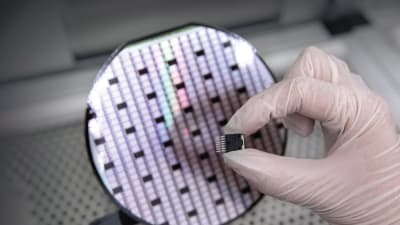
Articles: Semiconductors & ICs
See the products of tomorrow, including Lightmatter's chip specializing in AI operations and its interconnect that facilitates data transfer between chips; implantable biomedical devices; and a metallic nanotube.

INSIDER: Electronics & Computers
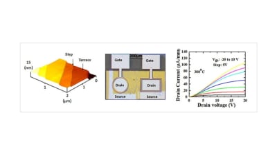
A NIMS research team has developed the world’s first n-channel diamond MOSFET. It provides a key step toward CMOS integrated circuits for harsh-environment applications as well as...
Blog: Green Design & Manufacturing
A process of heating carbon nitride to the required degree of crystallinity, maximizing the functional properties of this material for photocatalysis.

Articles: Software
As commercial fleets adopt more electric vehicles, they need accurate state-of-health measurements and smart charging algorithms to ensure their EVs have minimum unscheduled downtime. To solve these problems effectively, we need comprehensive data collection, capable computing infrastructure, and intelligent algorithms.

Articles: Energy
Currently, researchers are exploring the use of adhesives in combination with laser-cut gasket materials to deliver maximum energy density, miniaturization, and while maintaining a high degree of hermetic integrity to assure long-lived operation and efficiency.

Products: Electronics & Computers
See what's new on the market, including: new TEMPUS™ technology from Renishaw, SPIROL's Series CL6000 Compression Limiters, binder-USA's protective caps, a breakthrough lithium coin cell holder from Keystone Electronics, and more.

Products: Manufacturing & Prototyping
See the product of the month: The IMS5420-TH white light interferometer from Micro-Epsilon. The IMS5420-TH can be used for undoped, doped, and highly doped SI wafers.

Briefs: Electronics & Computers
A multi-institutional project led by a Penn State researcher is focused on developing an all-in-one semiconductor device that can both store data and perform computations. The project recently received $2 million in funding over three years as part of the new National Science Foundation Future of Semiconductors (FuSe) program.

Briefs: Photonics/Optics
RMIT University’s Arnan Mitchell and University of Adelaide’s Dr. Andy Boes led an international team to review lithium niobate’s capabilities and potential applications in the journal Science. The team is working to make navigation systems that help rovers drive on the Moon — where GPS is unable to work — later this decade.

INSIDER: Electronics & Computers
Moore's Law, a fundamental scaling principle for electronic devices, forecasts that the number of transistors on a chip will double every two years, ensuring more computing power —...
Briefs: Medical
This advancement, one of the first of its kind, enables a useful new capability for a variety of applications, including improved prostheses, haptics for new modalities in augmented reality (AR), and thermally modulated therapeutics for applications such as pain management. The technology also has a variety of potential industrial and research applications.

Briefs: Materials
The miniscule wires — the size of transistors on silicon chips or one thousandth of the breadth of the finest human hair — are made completely of natural amino acids and heme molecules, found in proteins such as hemoglobin, which transports oxygen in red blood cells.

INSIDER: Electronics & Computers
Scientists at the University of California San Diego and CEA-Leti have developed a ground-breaking piezoelectric-based DC-DC converter that unifies all power switches onto a single chip to...

Briefs: Manufacturing & Prototyping
Researchers have unveiled a remarkable new material with potential to impact the world of material science: amorphous silicon carbide (a-SiC). Beyond its exceptional strength, this material demonstrates mechanical properties crucial for vibration isolation on a microchip. It is therefore particularly suitable for making ultra-sensitive microchip sensors.
Briefs: Information Technology
Researchers have created a device that enables them to electronically steer and focus a beam of terahertz electromagnetic energy with extreme precision. This opens the door to high-resolution, real-time imaging devices that are hundredths the size of other radar systems and more robust than other optical systems.

Briefs: Manned Systems
Wireless power transfer was recently demonstrated by MAPLE — Microwave Array for Power-transfer Low-orbit Experiment — one of three key technologies being tested by the Space Solar Power Demonstrator (SSPD-1), the first space-borne prototype from Caltech’s Space Solar Power Project (SSPP), which aims to harvest solar power in space and transmit it to the Earth’s surface.

INSIDER: Materials
Researchers at the Georgia Institute of Technology have created the world’s first functional semiconductor made from graphene, a single sheet of carbon atoms held...

Top Stories
 Blog: Lighting
A Stretchable OLED that Can Maintain Most of Its Luminescence
 Blog: Energy
Batteries that Can Withstand the Cold
 INSIDER: Energy
Advancing All-Solid-State Batteries
 Blog: Power
My Opinion: We Need More Power Soon — Is Nuclear the Answer?
 Quiz: Power
 Blog: Data Acquisition
Webcasts
 Upcoming Webinars: Test & Measurement
From Spreadsheets to Insights: Fast Data Analysis Without Complex...
 Upcoming Webinars: Aerospace
Cooling a New Generation of Aerospace and Defense Embedded...
 Upcoming Webinars: Test & Measurement
Beyond AI-Copy-Paste Engineering: Advanced AI-Integration Success...
 Upcoming Webinars: Power
Battery Abuse Testing: Pushing to Failure
 Upcoming Webinars: AR/AI
A FREE Two-Day Event Dedicated to Connected Mobility
 Upcoming Webinars: RF & Microwave Electronics
Choosing the Right N-Port Strategy: Multiport VNAs vs. Switch...