Stories
54
0
930
30
Briefs: Semiconductors & ICs
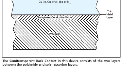
Improved low-resistance, semitransparent back contacts, and a method of fabricating them, have been developed for solar photovoltaic cells that are made from thin films of I-III-VI2...
Briefs: Electronics & Computers
A single-chip CMOS-based (complementary-metal-oxide-semi-conductor-based) transmit/receive (T/R) module is being developed for L-band radar systems. Previous T/R module implementations required multiple chips...

Briefs: Semiconductors & ICs
The figure is a schematic diagram of a complementary metal oxide/semiconductor (CMOS) electronic circuit that performs one of three different logic functions, depending on the level of an...

Briefs: Semiconductors & ICs
A circuit that changes an electrical load in a switching time shorter than 0.3 microsecond has been devised. This circuit can be used in testing the regulation characteristics of power-supply circuits...

Briefs: Semiconductors & ICs
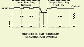
Figure 1 shows a single-stage monolithic microwave integrated circuit (MMIC) power amplifier in which the gain element is a double-heterojunction bipolar transistor (DHBT) connected in common-base...
Briefs: Semiconductors & ICs
A system of electronic instrumentation, constituting the equivalent of a two-port vector network analyzer, has been developed for use in on-wafer measurement of key electrical characteristics...
Briefs: Semiconductors & ICs
PVM Enhancement for Beowulf Multiple-Processor Nodes
A recent version of the Parallel Virtual Machine (PVM) computer program has been enhanced to enable use of multiple processors in a single node of a Beowulf system (a cluster of personal computers that runs the Linux operating system). A previous version of PVM had been enhanced by addition of a...
Briefs: Semiconductors & ICs
Programs for Testing Processor-in-Memory Computing Systems
The Multithreaded Microbenchmarks for Processor-InMemory (PIM) Compilers, Simulators, and Hardware are computer programs arranged in a series for use in testing the performances of PIM computing systems, including compilers, simulators, and hardware. The programs at the beginning of the...
Briefs: Semiconductors & ICs
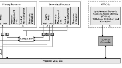
A fault-tolerant computer architecture has been conceived in an effort to reduce vulnerability to single-event upsets (spurious bit flips caused by impingement of energetic ionizing...
Briefs: Semiconductors & ICs
An improved apparatus has been designed and built for use in precise positioning and pressing of a microchip onto a substrate (which could, optionally, be another microchip) for the...

Briefs: Semiconductors & ICs
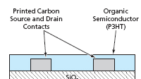
A low-temperature process for fabricating flexible, ohmic contacts for use in organic thin-film transistors (OTFTs) has been developed. Typical drainsource contact materials used...
Briefs: Semiconductors & ICs
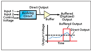
A modification in a method of automated evolutionary synthesis of voltage controlled multifunctional logic circuits makes it possible to synthesize more circuits in less time. Prior to the...
Briefs: Semiconductors & ICs
N-Type d Doping of High-Purity Silicon Imaging Arrays
A process for n-type (electron-donor) delta (d) doping has shown promise as a means of modifying back-illuminated image detectors made from n-doped high-purity silicon to enable them to detect high-energy photons (ultraviolet and x-rays) and low-energy charged particles (electrons and ions)....
Briefs: Semiconductors & ICs
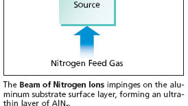
A technique based on accelerating positive nitrogen ions onto an aluminum layer has been demonstrated to be effective in forming thin (<2 nm thick) layers of aluminum nitride...
Briefs: Semiconductors & ICs
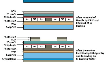
A process that employs silicon-on-insulator (SOI) substrates and silicon (Si) micromachining has been devised for fabricating wide intermediate frequency band (wide-IF) superconductor/...
Briefs: Semiconductors & ICs
Advanced packaging techniques are the key to utilizing state-of-the-art microelectronic devices. The flip-chip method has become a cost-effective means of erasing many...
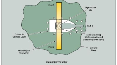
Briefs: Semiconductors & ICs
A stripline to microstrip transition has been incorporated into a multilayer circuit board that supports a distributed solid-state microwave power amplifier, for the purpose of...
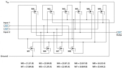
Briefs: Software
The figure is a schematic diagram of a complementary metal oxide/semiconductor (CMOS) electronic circuit that functions as a NAND gate at a power-supply potential (Vdd) of 3.3 V and as NOR...
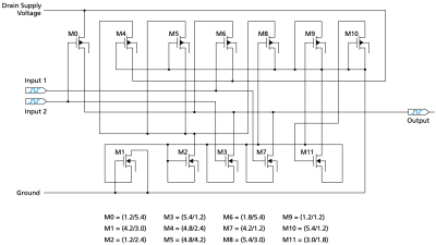
Briefs: Semiconductors & ICs
The figure is a schematic diagram of a complementary metal oxide/semiconductor (CMOS) electronic circuit that has been designed to function as a NAND gate at a temperature between 0 and 80...
Briefs: Semiconductors & ICs
LC Circuits for Diagnosing Embedded Piezoelectric Devices
A recently invented method of nonintrusively detecting faults in piezoelectric devices involves measurement of the resonance frequencies of inductor-capacitor (LC) resonant circuits. The method is intended especially to enable diagnosis of piezoelectric sensors, actuators, and...
Briefs: Semiconductors & ICs
Improved Method of Manufacturing SiC Devices
The phrase, "common-layered architecture for semiconductor silicon carbide" ("CLASSiC") denotes a method of batch fabrication of microelectromechanical and semiconductor devices from bulk silicon carbide. CLASSiC is the latest in a series of related methods developed in recent years in continuing efforts...
Briefs: Semiconductors & ICs
An active frequency doubler in the form of an InP-based monolithic microwave integrated circuit (MMIC) containing a high electron mobility transistor (HEMT) has been demonstrated in operation at...
Briefs: Semiconductors & ICs
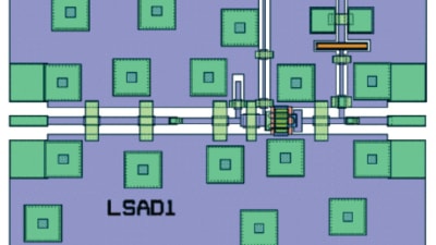
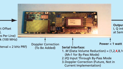
A field-programmable gate array (FPGA) on a single lightweight, low power integrated-circuit chip has been developed to implement an azimuth pre-filter (AzPF) for a synthetic-aperture radar (SAR)...
Briefs: Semiconductors & ICs
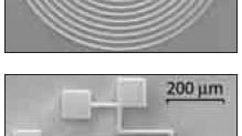
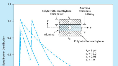
Ribbon waveguides made of alumina or of semiconductors (Si, InP, or GaAs) have been proposed as low-loss transmission lines for coupling electronic components and circuits that...
Briefs: Electronics & Computers
Electronic heat-transfer devices of a proposed type would exploit some of the quantum-wire-like, pseudo-superconducting properties of single-wall carbon nanotubes or, optionally, room- temperature-...

Briefs: Semiconductors & ICs
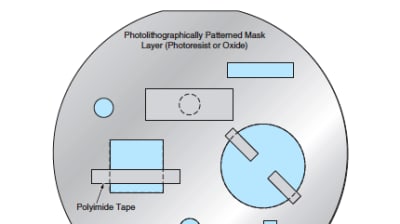
Polyimide tape (Kapton™ or equivalent) has been found to be effective as a material for masking selected areas of a semi- conductor wafer that is about to be processed in a...
Briefs: Semiconductors & ICs
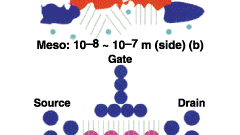
Since its invention in 1948, the transistor has revolutionized everyday life. The electronics revolution is based on miniaturization of transistors; smaller transistors are faster, and...
Briefs: Sensors/Data Acquisition
Active-pixel integrated-circuit image sensors that can be programmed in real-time to effect artificial reconfigurable vision on demand have been developed and demonstrated. In...

Briefs: Semiconductors & ICs
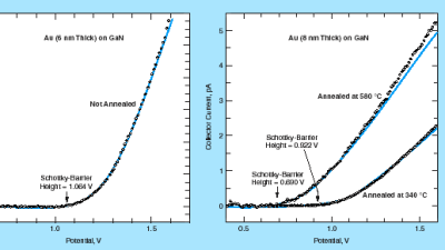
Annealing has been found to be an effective means of tailoring the height of a Schottky barrier between gold and gallium nitride. This finding offers promise for the development of improved...
Top Stories
 Blog: Lighting
A Stretchable OLED that Can Maintain Most of Its Luminescence
 Blog: Energy
Batteries that Can Withstand the Cold
 INSIDER: Energy
Advancing All-Solid-State Batteries
 Blog: Power
My Opinion: We Need More Power Soon — Is Nuclear the Answer?
 Quiz: Power
 Blog: Data Acquisition
Webcasts
 Upcoming Webinars: Test & Measurement
From Spreadsheets to Insights: Fast Data Analysis Without Complex...
 Upcoming Webinars: Aerospace
Cooling a New Generation of Aerospace and Defense Embedded...
 Upcoming Webinars: Test & Measurement
Beyond AI-Copy-Paste Engineering: Advanced AI-Integration Success...
 Upcoming Webinars: Power
Battery Abuse Testing: Pushing to Failure
 Upcoming Webinars: AR/AI
A FREE Two-Day Event Dedicated to Connected Mobility
 Upcoming Webinars: RF & Microwave Electronics
Choosing the Right N-Port Strategy: Multiport VNAs vs. Switch...