
Artifacts that are fabricated with the help of molecular-beam epitaxy (MBE) are undergoing development for use as dimensional calibration standards with sub-micron widths. Such standards are needed for calibrating instruments (principally, scanning electron microscopes and scanning probe microscopes) for measuring the widths of features in advanced integrated circuits. Dimensional calibration standards fabricated by an older process that involves lithography and etching of trenches in (110) surfaces of single-crystal silicon are generally reproducible to within dimensional tolerances of about 15 nm. It is anticipated that when the artifacts of the present type are fully developed, their critical dimensions will be reproducible to within 1 nm. These artifacts are expected to find increasing use in the semiconductor-device and integrated-circuit industries as the width tolerances on semiconductor devices shrink to a few nanometers during the next few years.
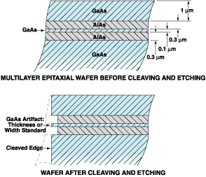
Unlike in the older process, one does not rely on lithography and etching to define the critical dimensions. Instead, one relies on the inherent smoothness and flatness of MBE layers deposited under controlled conditions and defines the critical dimensions as the thicknesses of such layers. An artifact of the present type is fabricated in two stages (see figure): In the first stage, a multilayer epitaxial wafer is grown on a very flat substrate. In the second stage, the wafer is cleaved to expose the layers, then the exposed layers are differentially etched (taking advantage of large differences between the etch rates of the different epitaxial layer materials).
The resulting structure includes narrow and well-defined trenches and a shelf with thicknesses determined by the thicknesses of the epitaxial layers from which they were etched. Eventually, it should be possible to add a third fabrication stage in which durable, electronically inert artifacts could be replicated in diamond-like carbon from a master made by MBE and etching as described above.
This work was done by Frank Grunthaner and Paula Grunthaner of Caltech and Charles Bryson III of Surface/Interface, Inc., for NASA's Jet Propulsion Laboratory. For further information, access the Technical Support Package (TSP) free on-line at www.techbriefs.com/tsp under the Information Sciences category.
In accordance with Public Law 96-517, the contractor has elected to retain title to this invention. Inquiries concerning rights for its commercial use should be addressed to:
Intellectual Property group
JPL
Mail Stop 202-233
4800 Oak Grove Drive
Pasadena, CA 91109
(818) 354-2240
Refer to NPO-21130, volume and number of this NASA Tech Briefs issue, and the page number.
This Brief includes a Technical Support Package (TSP).
Artifacts for Calibration of Submicron Width Measurements
(reference NPO-21130) is currently available for download from the TSP library.
Don't have an account?
Overview
The document is a technical support package from NASA's Jet Propulsion Laboratory (JPL) detailing the development of artifacts for calibrating submicron width measurements, specifically aimed at improving the accuracy of semiconductor manufacturing. The report outlines the innovative approach taken to create a reproducible width artifact that can meet the stringent demands of modern semiconductor technology, where tolerances are rapidly decreasing.
The proposed solution involves a two-step fabrication process. The first step is to create a multilayer structure by epitaxially growing layers on a very flat substrate. The second step involves exposing these layers by fracturing the wafer and using differential etching to form narrow, well-defined trenches. The widths of these trenches are determined by the thickness of the epitaxial layers, allowing for precise control over the dimensions. The final artifacts may be replicated in diamond-like carbon to ensure durability and resistance to corrosion, which is essential for long-term use in semiconductor applications.
The document highlights the limitations of current measurement tools, such as electron-beam-based tools and scanning probe microscopes, which suffer from various sources of error, including electron scattering and tip shape determination. These issues can lead to inaccuracies in measuring the dimensions of semiconductor features. The new artifacts aim to provide a reliable external standard that can help reduce calibration errors and improve measurement precision across different instruments.
The report emphasizes the novelty of the MBE Critical Dimension Artifact, which utilizes ultra-flat surfaces and controlled film depositions to achieve unprecedented reproducibility. Current technologies are limited by the capabilities of lithography and etching processes, which can only achieve reproducibility down to about 15 nanometers. The new approach aims to push this limit down to 1 nanometer, addressing the industry's need for accuracy as semiconductor width tolerances are expected to drop to 2-3 nanometers in the near future.
Overall, the document outlines a significant advancement in the field of semiconductor measurement, providing a foundation for improved calibration techniques that can enhance the precision and reliability of semiconductor manufacturing processes.